Nano Res.[探测]│南京航空航天大学郭万林院士团队聂日明教授课题组:溶液法 Pb₂SbS₂I₃薄膜实现单次曝光双能 X 射线成像
- 2026-05-24 01:53:41

背景介绍
X 射线成像因其非侵入式的内部结构可视化能力,被广泛应用于医疗诊断、安检与工业无损检测等场景。然而,常规 X 射线成像往往缺乏能量分辨能力:不同材料对不同能量 X 射线的吸收差异被“压缩”到单一灰度信号中,导致材料区分度受限。
为提升材料区分能力,双能 X 射线成像(DEXI)通过获取低能与高能两类信息实现能量维度的互补。但现有 DEXI 方案通常依赖多次曝光或复杂、昂贵的能量分辨读出(如光子计数体系),在成本、结构复杂度与可扩展性方面仍存在掣肘。此外,在常见 X 射线管的轫致辐射谱中,低能(软)X 射线成分客观存在,却往往在常规探测中被高能信号“淹没”,难以被有效提取并用于成像。
成果简介
本工作提出一种“探测式滤光片”思路:在现有探测器前端引入一层可直接探测软 X 射线的吸收层,一方面将软 X 射线信息从混合信号中分离出来,另一方面允许高能 X 射线穿透并由后端常规探测器继续采集,从而在单次曝光中获得互补的能量信息。
我们首次将金属硫卤化物 Pb2SbS2I3应用于 X 射线探测,利用其较高的原子序数与密度,在约 20 μm 厚度下即可实现对 <10 keV 软 X 射线的强吸收,同时对高能 X 射线保持较高透过性。基于溶液法制备的 Pb2SbS2I3 直接型软 X 射线探测器在低偏压下表现出优异综合性能:灵敏度可达 9669 μC·Gyair−1·cm−2,最低检测限低至 71 nGyair·s−1,并具备毫秒级响应(0.7 ms/1.6 ms,上升/下降)。进一步地,将 Pb2SbS2I3 前端层与后端钙钛矿/商用探测器协同集成,可在不改变后端探测器工作方式的前提下实现单次曝光双能成像示范,为在现有成像体系中“捡回”软 X 射线信息提供了模块化、低成本的实现路径。
本研究第一作者为南京航空航天大学博士研究生朱冰鉴,通讯作者包括郭万林院士、张助华教授、聂日明教授和雷威教授,工作由南京航空航天大学与东南大学团队联合完成。
图文导读
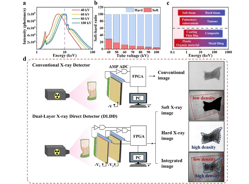
Figure 1. Design Rationale for the Dual-Energy X-Ray Detector. (a) Simulated bremsstrahlung spectra of a conventional gold-target X-ray tube under various tube voltages (40–100 kV). (b) The proportion of soft X-rays (below 10 keV) generated at different tube voltages. (c) X-ray energy ranges suitable for detecting different materials. (d) Schematic of the conceptual imaging process for a conventional single-layer X-ray detector and our proposed dual-layer detector architecture.
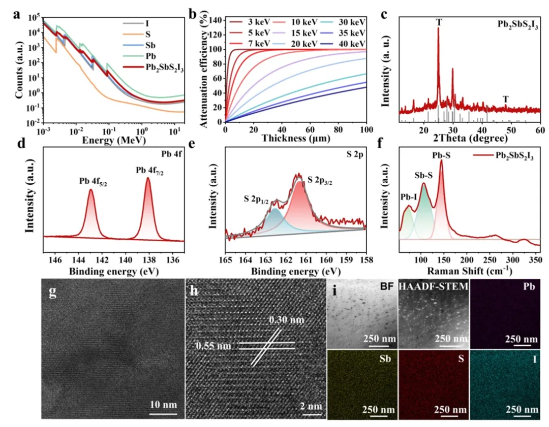
Figure 2. Structural and Chemical Characterization of Pb2SbS2I3 for Soft X-Ray Absorption. (a) Simulated X-ray absorption characteristics of Pb2SbS2I3. (b) The ability of Pb2SbS2I3 with various thickness to absorb X-rays. (c) XRD pattern of the optimized Pb2SbS2I3 film. (d) High resolution XPS spectrum of Pb 4f. (e) High resolution XPS spectrum of S 2p. (f) Raman spectrum of Pb2SbS2I3. (g) HRTEM image at 10 nm scale showing well-defined lattice fringes in Pb2SbS2I3. (h) HRTEM image at 2 nm scale, showing lattice spacings of 0.55 nm horizontally and 0.30 nm diagonally. (i) EDS maps showing the uniform distribution of Pb, Sb, S, and I in the Pb2SbS2I3 film, along with BF and HAADF-STEM images at 250 nm scale.
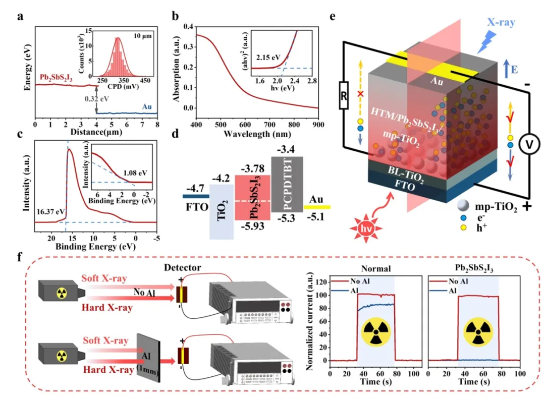
Figure 3. Device Structure Characterization of Pb2SbS2I3. (a) Kelvin probe force microscopy (KPFM) surface potential mapping of Pb2SbS2I3. (b) UV-Vis absorption spectrum of Pb2SbS2I3. Inset: Tauc plot analysis indicating a bandgap of 2.15 eV. (c) Ultraviolet photoelectron spectroscopy (UPS) of Pb2SbS2I3. Inset: magnified region indicating an onset of 1.08 eV. (d) Schematic energy level diagram of the device structure. (e) Cross-sectional device structure schematic of the X-ray detector. (f) Comparison of normalized photocurrent response of Pb2SbS2I3 and normal detectors with and without an Al filter to block soft X-rays.
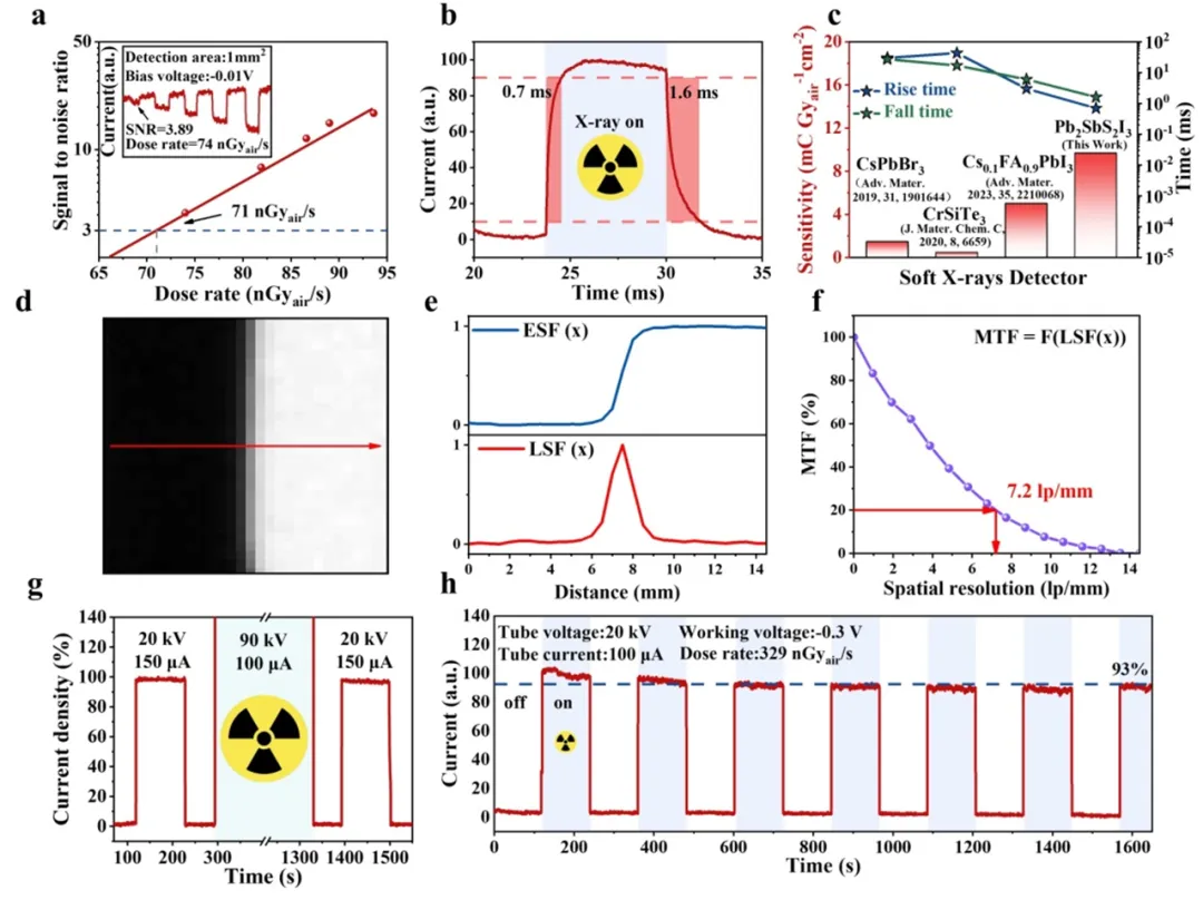
Figure 4. Device Performance of Pb2SbS2I3-based X-ray Detectors. (a) Minimum detection limit for the optimized 1.3 mol/L device. (b) Response time measurements showing a rise time of 0.7 ms and fall time of 1.6 ms. (c) Performance comparison with existing soft X-ray detectors. (d) Setup for resolution testing using stepwise scanning across a metal edge. (e) Edge spread function (ESF). Line spread function (LSF). (f) Modulation transfer function (MTF) plot showing a resolution of 7.2 lp/mm at 20% contrast threshold. (g) Radiation stability test after 20 minutes of high-energy X-ray exposure. (h) Stability testing under continuous unencapsulated X-ray exposure at 20 kV and 100 µA.
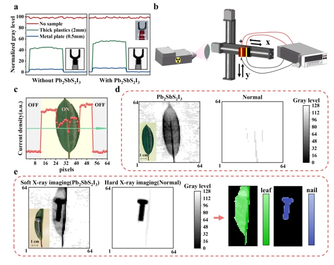
Figure 5. Enhanced Dual-Energy Imaging with Pb2SbS2I3-based Soft X-ray Detection. (a) Normalized current response line plots for X-ray imaging with and without a Pb2SbS2I3 detector. The left plot represents the conventional X-ray detector image without Pb2SbS2I3 detector while the right plot includes the Pb2SbS2I3 detector. (b) Schematic of rail-guided dual-detector imaging system. (c) Line plot of signal intensity along the center line of a scanned leaf structure. (d) Comparison of Pb2SbS2I3 and normal detector images of a leaf. (e) Dual-energy imaging results for a composite leaf and nail object, showing the soft X-ray detector image (left), hard X-ray detector image (middle), and a dual-energy subtraction image (right), with color mapping distinguishing the leaf in green and the nail in blue.
作者简介
聂日明教授为南京航空航天大学教授、博士生导师,主要从事空天能源与探测相关研究,包括钙钛矿/金属硫族-卤族化合物器件、光电探测器与 X 射线探测等方向。
招生信息:课题组招收钙钛矿/金属硫族-卤族化合物太阳能电池方向硕士研究生 2–3 名、博士研究生 1–2 名,并招收博士后及研究助理若干名;联系邮箱:rmnie@nuaa.edu.cn。
文章信息
Zhu B, Li Y, Chu W, et al. Solution-processed Pb2SbS2I3 for soft X-ray detection and single-exposure dual-energy imaging. Nano Research, 2026, 19(3): 94908288. https://doi.org/10.26599/NR.2025.94908288.

识别二维码或点击左下角“阅读原文”可访问全文

随机文章
-
 10个月宝宝每天需要喝多少奶粉?
- 美翻了,我的村!| 江苏省南京市龙尚村:碧水龙尚物产丰
- 热烈庆祝南京 — 巴黎洲际航线盛大开航
- 巾帼展英姿,冰壶竞芳华——南京盲校女教职工旱地冰壶活动掠影
- 联环(南京)召开2026年度股东会暨第三届第五次董事会
- 茅台酒╮五粮液╮威士忌洋酒收酒上门回收,南京高价回收老酒╰满足您的换酒需求!
- 【10】2026江苏南京七校高三联合体联考-PPT+word(免费下载)
- 南京晶丽海鲜自助餐厅(新街口IFCX店)3月-5月特惠!工作日午餐160/位 晚餐及周末¥175/位.生日当日赠送生日蛋糕.
- 为什么说2025年报考南京大学大气科学的浙江考生,都是“懂行的”?
- 【南京丨枕松度假酒店】¥399起/24-30㎡松字房木屋标间1晚,含2大1小(1.4米以下)早餐+松林岛屿+垂钓等
- 2026南京高中招生信息登记与联系方式汇总(3月11日)
